Introduction to DDIC (Display Driver IC)

What is DISPLAY DRIVER?
Executive Summary: Display Driver ICs in 2026
Quick Answer: A Display Driver IC (DDIC) is the essential semiconductor component acting as the "brain" of a screen. It translates digital signals from the device's processor into analog voltage to control pixel brightness and color. In 2026, DDICs are critical for enabling 120Hz+ variable refresh rates (LTPO), 8K resolution, and ultra-thin bezels in OLED and Micro-LED devices.
Key Takeaways:
Function: Controls Gate and Source lines to render images via T-CON coordination.
Tech Types: Active Matrix (AMOLED) is the standard for high-performance displays; Passive Matrix (PMOLED) is reserved for low-cost wearables.
Packaging: COP (Chip on Plastic) enables the foldable and bezel-less designs seen in modern flagships, succeeding legacy COG and COF methods.
Catalog |
Display Driver IC (DDIC) serves as the fundamental control component of modern panels, effectively operating as the "brain" of the display interface. As of 2026, its primary function is to transmit precise drive signals and video data to the display panel via electrical impulses. By regulating screen brightness, contrast, and color depth at the pixel level, the DDIC ensures that text, high-resolution images, and videos are rendered with high fidelity.
I What is a DDIC in modern electronics?
A Display Driver Integrated Circuit (DDIC) is a semiconductor device that controls the display pixels on screens ranging from smartphones to automotive dashboards. In the context of 2026 technology, the DDIC is crucial for managing the OLED and Micro-LED panels found in high-end devices. It must facilitate thin, flexible, and foldable form factors while delivering wide color gamuts (DCI-P3/Rec.2020) and managing high refresh rates (up to 144Hz or 240Hz). Crucially, modern DDICs are optimized for energy efficiency, utilizing LTPO technology to lower power consumption compared to legacy LCDs, thereby extending battery life.

OLED DDIC: Controlling the pixel sub-structure
The DDIC drives the display panel through electrical signals and transmits video data. The architecture of the DDIC differs significantly depending on whether it drives a PMOLED (Passive Matrix) or AMOLED (Active Matrix) panel:
In PMOLED: The DDIC inputs current to both horizontal and vertical ports. Pixel dots light up under current excitation, with brightness controlled by the current level. This is now mostly used in low-cost wearables.
In AMOLED (Industry Standard): Each pixel corresponds to a TFT layer (Thin Film Transistor) and a data storage capacitor. The DDIC controls the gray level of each pixel individually via the TFT. This approach achieves superior power efficiency and lifespan. Each pixel comprises sub-pixels representing the RGB (Red, Green, Blue) spectrum.
The voltage value (or On-state duty cycle) is transmitted sequentially in a scanning rhythm. The ICs responsible for this scanning are divided into two categories:
Gate IC (Row IC): Responsible for horizontal activation (switching lines on/off).
Source IC (Column IC): Responsible for vertical data voltage (determining pixel color/brightness).

DDIC Location on Panel

Architecture: Gate Driver, Source Driver, and TCON
The Challenge of Large Screens: OLED DDICs for large displays (TVs/Monitors) face challenges due to the non-uniformity of LTPS (Low-Temperature Poly-Silicon) material. As screens scale up, signal propagation delay can cause image tearing. Advanced 2026 DDICs use compensation algorithms: they store a "map" of the TFT nonuniformity and adjust signals dynamically to ensure a uniform picture.
The Role of the T-CON: DDICs require a supervisor chip called the Timing Controller (T-CON). Often considered the "CPU" of the display, the T-CON analyzes signals from the host (GPU/Motherboard), converts them into a format the Source/Gate ICs understand, and manages timing precision. With the rise of 4K, 8K, and VR/AR resolutions, the T-CON's processing power is vital for managing massive bandwidth and ensuring fluid refresh rates.
II How do Passive Matrix and Active Matrix differ?
Active Matrix (AMOLED) controls pixels individually using local capacitors for sustained brightness, whereas Passive Matrix (PMOLED) relies on high-speed line scanning, which limits resolution.
In a basic matrix, adding voltage to specific rows and columns lights up the intersection. However, a major issue arises: if we attempt to light up pixels 2B and 5E simultaneously, the intersecting voltages might inadvertently light up 5B and 2E (a phenomenon known as "crosstalk" or "ghosting").
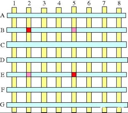
Display Matrix Structure
The Passive Matrix Solution: The system processes one X-axis line at a time. It applies voltage to one horizontal line, scans all Y-axis values, and quickly switches to the next line. Due to the "persistence of vision" effect, if this scanning happens fast enough, the human eye perceives a complete image. However, this has significant downsides in 2026 standards:
Low Brightness: Pixels are only "on" for a fraction of a second during their scan line time.
Signal Bleed: Activation of one pixel can slightly affect neighbors, resulting in blurred edges and poor definition.
How does Active Matrix solve this?
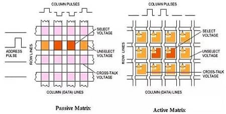
Circuit Comparison: Active Matrix vs. Passive Matrix
Active Matrix adds a switch (TFT) and a capacitor to every single pixel.
Energy Conservation: When the scan line passes, the capacitor charges and holds the voltage. This keeps the pixel lit continuously until the next refresh cycle, drastically increasing brightness and contrast.
Isolation: The transistor acts as a precise gate. Voltage applied to one pixel is isolated, preventing "crosstalk" with neighboring pixels.
This architecture is the foundation of AMOLED. While AM technology increases manufacturing complexity and cost, it is essential for the high-resolution, high-contrast screens demanded by today's users.
III What are COG, COF, and COP Packaging Technologies?
Packaging technology determines how the DDIC connects to the display panel, directly influencing the bezel width and the device's "screen-to-body" ratio.
Since the introduction of flexible displays (popularized by Samsung and widely adopted in 2026 foldables), packaging has evolved. Broadly, displays are Rigid (glass substrate) or Flexible (polyimide/plastic substrate). The three primary packaging methods are:
1. COG (Chip On Glass)
The DDIC is bonded directly onto a rigid glass substrate. This is the legacy standard for budget LCDs. Because the chip sits on the glass, it requires a larger bottom bezel ("chin") to accommodate the chip and the FPCB connection.

COG Cross-section
2. COF (Chip On Film)
The DDIC is bonded to a flexible FPCB (film) rather than the glass itself. This film can be folded behind the panel, reducing the module's bottom edge by approximately 1.5mm. COF is common in mid-range smartphones and tablets.
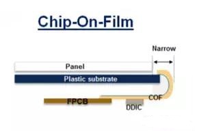
COF Cross-section
3. COP (Chip On Plastic)
The premium standard for 2026. Because OLEDs use a flexible plastic substrate, the substrate itself—containing the DDIC—can be bent completely backward. This allows the driver circuits to be tucked underneath the display area, enabling near-zero bottom bezels. This technology is utilized in flagship devices like the latest iPhone Pro series and Samsung Galaxy S series.
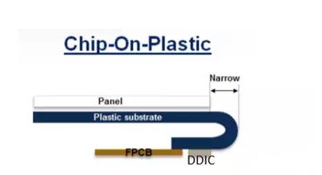
COP Cross-section
Visualizing the Difference:
In a standard COG LCD module, the "chin" includes the dispensing area, the FPC line, and the Driver IC sitting on the glass. This results in a thick bottom bezel.
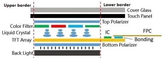
Legacy LCD Module Structure
In COF, moving the driver IC to the flexible film allows the connection area to be folded, significantly shrinking the chin. This is a staple for cost-effective Android devices.
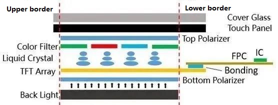
LCD Module with COF Packaging
Finally, COP leverages the flexibility of the OLED's plastic substrate. By bending the substrate itself, the connection area essentially disappears from the front view. This explains why modern flagships have uniform bezels on all four sides.
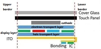
COP Packaging Principle (OLED)
1.What does display driver IC do?
A display driver is a type of semiconductor with an integrated circuit that acts as an interface between microprocessors and LCDs. The device controls display systems in PCs and cell phones. The display driver IC market is divided into two broad segments, namely the LED DDIC and touches controller IC (TCIC).
2.What is one of the main control components of the panel?
Display Driver IC
3.What is the source IC also called?
Column IC
4.What drives the display by scanning?
The DDIC
5.What type of material does flexible screens use as the substrate?
Plastic
 Discovering New and Advanced Methodology for Determining the Dynamic Characterization of Wide Bandgap DevicesSaumitra Jagdale15 March 20242470
For a long era, silicon has stood out as the primary material for fabricating electronic devices due to its affordability, moderate efficiency, and performance capabilities. Despite its widespread use, silicon faces several limitations that render it unsuitable for applications involving high power and elevated temperatures. As technological advancements continue and the industry demands enhanced efficiency from devices, these limitations become increasingly vivid. In the quest for electronic devices that are more potent, efficient, and compact, wide bandgap materials are emerging as a dominant player. Their superiority over silicon in crucial aspects such as efficiency, higher junction temperatures, power density, thinner drift regions, and faster switching speeds positions them as the preferred materials for the future of power electronics.
Read More A Comprehensive Guide to FPGA Development BoardsUTMEL11 September 202514677
This comprehensive guide will take you on a journey through the fascinating world of FPGA development boards. We’ll explore what they are, how they differ from microcontrollers, and most importantly, how to choose the perfect board for your needs. Whether you’re a seasoned engineer or a curious hobbyist, prepare to unlock new possibilities in hardware design and accelerate your projects. We’ll cover everything from budget-friendly options to specialized boards for image processing, delve into popular learning paths, and even provide insights into essential software like Vivado. By the end of this article, you’ll have a clear roadmap to navigate the FPGA landscape and make informed decisions for your next groundbreaking endeavor.
Read More Applications of FPGAs in Artificial Intelligence: A Comprehensive GuideUTMEL29 August 20253607
This comprehensive guide explores FPGAs as powerful AI accelerators that offer distinct advantages over traditional GPUs and CPUs. FPGAs provide reconfigurable hardware that can be customized for specific AI workloads, delivering superior energy efficiency, ultra-low latency, and deterministic performance—particularly valuable for edge AI applications. While GPUs excel at parallel processing for training, FPGAs shine in inference tasks through their adaptability and power optimization. The document covers practical implementation challenges, including development complexity and resource constraints, while highlighting solutions like High-Level Synthesis tools and vendor-specific AI development suites from Intel and AMD/Xilinx. Real-world applications span telecommunications, healthcare, autonomous vehicles, and financial services, demonstrating FPGAs' versatility in mission-critical systems requiring real-time processing and minimal power consumption.
Read More 800G Optical Transceivers: The Guide for AI Data CentersUTMEL24 December 20253831
The complete guide to 800G Optical Transceiver standards (QSFP-DD vs. OSFP). Overcome supply shortages and scale your AI data center with Utmel Electronic.
Read More Xilinx FPGAs: From Getting Started to Advanced Application DevelopmentUTMEL09 September 20254299
This guide is your comprehensive roadmap to understanding and mastering the world of Xilinx FPGA technology. From selecting your first board to deploying advanced AI applications, we'll cover everything you need to know to unlock the potential of these remarkable devices. The global FPGA market is on a significant growth trajectory, expected to expand from USD 8.37 billion in 2025 to USD 17.53 billion by 2035. This surge is fueled by the relentless demand for high-performance, adaptable computing in everything from 5G networks and data centers to autonomous vehicles and the Internet of Things (IoT). This guide will walk you through the key concepts, tools, and products in the Xilinx ecosystem, ensuring you're well-equipped to be a part of this technological revolution.
Read More
Subscribe to Utmel !
![UCC5310MCDR]() UCC5310MCDR
UCC5310MCDRTexas Instruments
![1EDI20H12AHXUMA1]() 1EDI20H12AHXUMA1
1EDI20H12AHXUMA1Infineon Technologies
![1EDI60H12AHXUMA1]() 1EDI60H12AHXUMA1
1EDI60H12AHXUMA1Infineon Technologies
![1EDI30I12MFXUMA1]() 1EDI30I12MFXUMA1
1EDI30I12MFXUMA1Infineon Technologies
![UCC21220DR]() UCC21220DR
UCC21220DRTexas Instruments
![HCS201T-I/SN]() HCS201T-I/SN
HCS201T-I/SNMicrochip Technology
![ADATE305BSVZ]() ADATE305BSVZ
ADATE305BSVZAnalog Devices Inc.
![AD9172BBPZ]() AD9172BBPZ
AD9172BBPZAnalog Devices Inc.
![ADUM4223CRWZ]() ADUM4223CRWZ
ADUM4223CRWZAnalog Devices Inc.
![FM33256B-G]() FM33256B-G
FM33256B-GCypress Semiconductor Corp


 Product
 Brand
Brand Articles
 Tools
Tools


